

PCB Layout Design
The design of a printed circuit board (PCB), is certainly one of the most complex operations that the designer has to face, being both an art and a science. It requires a careful assessment of the space available on the board and the constraints imposed by the circuit and components. Creating a reliable, functional and cost effective PCB designs is a challenge, especially today when the need is to create compact, light and sometimes even flexible boards.
The design flow of a printed circuit always starts from the schematic, followed by the positioning of the components, the definition of the layers and the traces, and ends with the generation of Gerber files. The process of defining the traces, also known as routing, can be performed in different ways: manual, automatic, or interactive (a combination of the previous two).
The more complex the card applications are, the more appropriate the manual routing technique is. Elenos is experienced in several types of designs:
- RF boards, which may require transmission lines (microstrip, stripline, or others) and where the impedance value must be strictly controlled in order to avoid power losses and guarantee signal integrity;
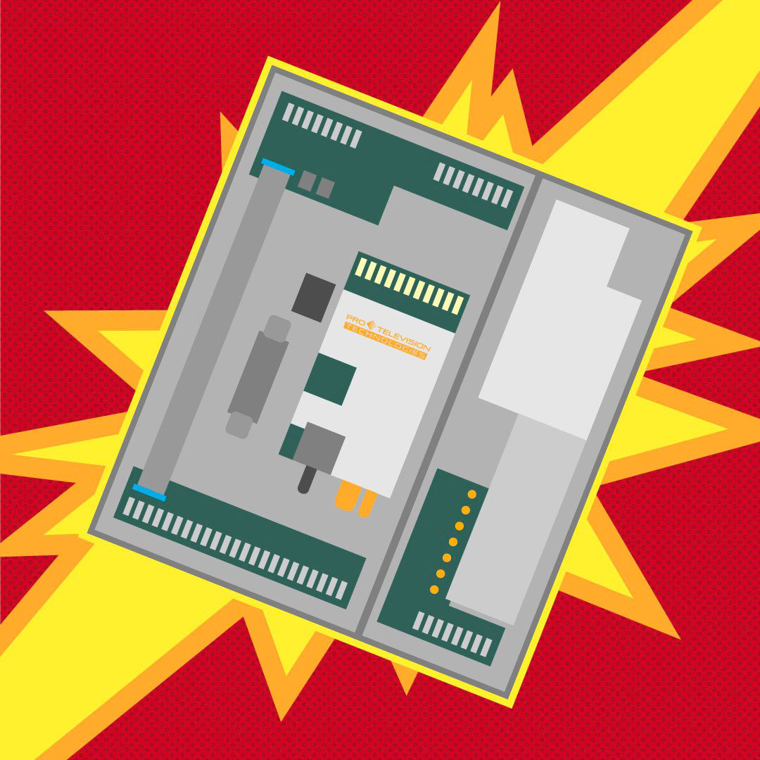
- Power Supplies, where safety and efficiency are critical and everything from insulation to thermal management must be considered. Additionally, power supplies tend to have physical constraints imposed by the enclosure and heatsinks which need to be considered so the manual routing technique is typically used.
Manual routing is the one that offers creative professional satisfaction, but it requires time and patience. It consists in manually positioning the traces that connect the components, defining technical characteristics such as thickness, width, distance and angle of curvature. The designer is certainly aided by the software tool, which is capable of reporting any violations of the routing rules, but the designer’s skill and competence is paramount.
Fully automatic routing, on the other hand, operates completely autonomously – once the routing rules are established, the project is automatically processed by the systemand the result can then be revised by manually making any necessary changes or improvements. Although autorouting is a technique that can save the time, it is not necessarily the one provides the best results. Like all automated processing systems, autorouting has its limitations and, despite the advances in the software tools, it is regarded by some as difficult to configure for optimal results, and the designer may have to correct the automatically created routing, fixing common errors such as traces going around the edges of the PCB, rather than traversing the layers. It is therefore essential to know the limits of application of each technique and to evaluate when one is preferable over the others.
Finally, interactive routing is a technique that combines the precision and control of manual routing with the speed and automation typical of autorouting.
Regardless of the methodology used, routing presents a complexity that increases with the number of components present on the board and remains particularly critical in applications where there are high frequency signals or there are components which must dissipate significant heat.
In the broadcast transmitter field, the PCB characteristics that lead our designers to prefer the manual routing technique are:
- Traces of reduced length: if the distance between the pins to be connected is very small, manual routing is the technique that produces the most reliable and accurate results; in addition to being satisfying, it can be performed almost mechanically;
- The angle of the traces: 90° angles should be avoided as, during manufacturing, the etching process could create dangerous short circuits; sharp angles should also be avoided. Working manually, the designer can model the trace by applying the appropriate degree of curvature;
- Highly complex circuits: where the density of components and numerous interconnections require special attention. In these cases, the experienced designer can can often create a superior design versus an automatic tool.
PCB Layout Designers at Elenos have:
- Great attention to detail: when the job involves finding solutions with minimal adjustment changes, or when working with microscopic materials, it is essential to have an eye for detail;
- Ability to constantly update: in a constantly evolving sector such as technology, and with the appearance of new and more efficient and intelligent software, not updating means risking being left behind;
- Ability to learn new design techniques: perhaps it seems obvious, but after years of work it is easy to become habitual, always falling back on the same tried and tested layout techniques. But this can encourage repeated mistakes, or lead to new ones, as layouts become more complex;
- Ability to work for long periods of time: Experience is key, the pressures of timelines must be resisted to assure consistant quality.
- Problem solving and mediation skills: The PCB design process involves many partners, and often, PCB design ends up being a tug-of-war between engineering and manufacturing, and it is up to the designer to find a solution that satisfies both sides.


